New collaboration with chip R&D lab New York CREATES will focus on extreme ultraviolet (EUV) lithography and metrology techniques.
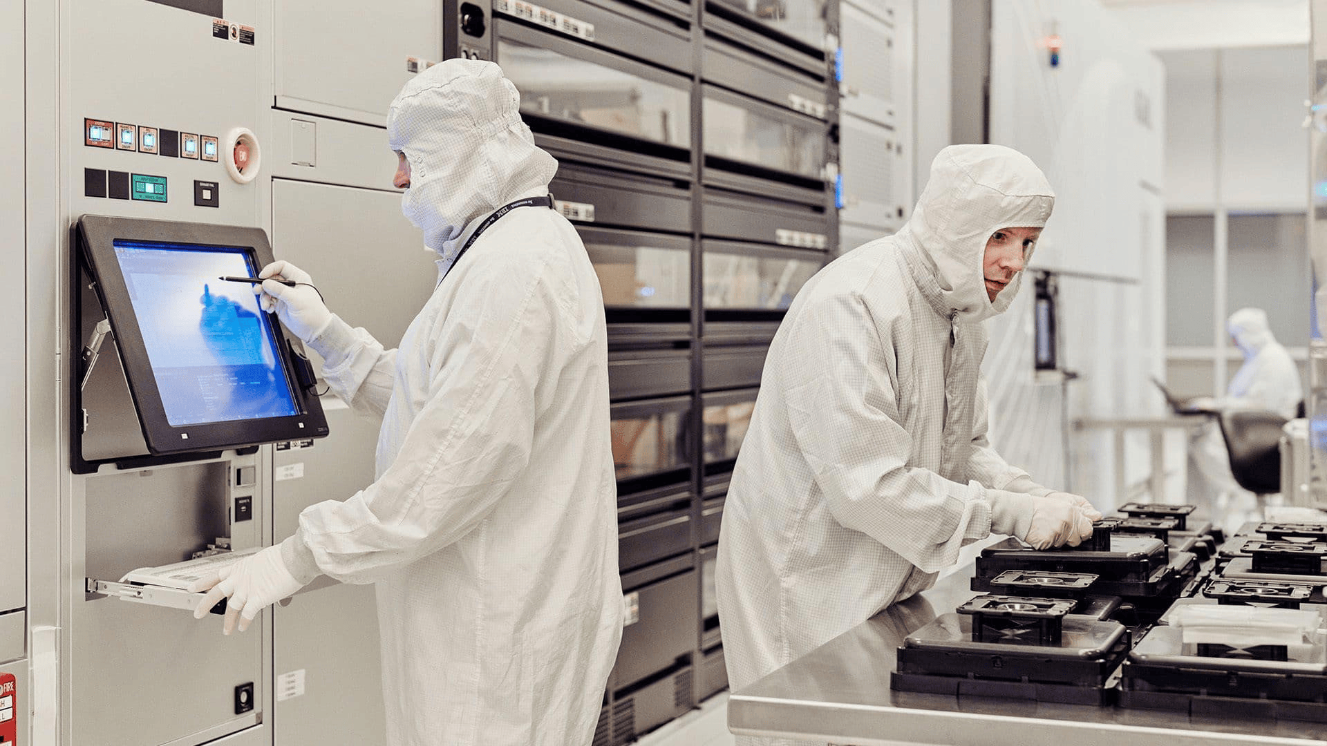
The race for global leadership in semiconductor manufacturing is about more than building new fabrication facilities. It is also about developing the scientific capabilities, advanced materials, and manufacturing processes necessary to produce the next generation of microchips.
A new partnership between the semiconductor R&D lab NY CREATES and two DOE national labs, Brookhaven and Lawrence Berkeley, represents an important step toward strengthening America’s semiconductor innovation ecosystem.
Launched on November 5, 2026, the collaboration establishes a pilot program funded by the U.S. Department of Energy’s Office of Science to connect semiconductor manufacturers with world-class scientific research facilities and expertise. The initiative is designed to accelerate technological breakthroughs, address critical manufacturing challenges, and shorten the path from scientific discovery to commercial application.
From Leading Edge Research to New Energy Efficient Chips
One of the persistent challenges facing the U.S. semiconductor industry is translating advances in fundamental research into practical manufacturing technologies.
Developing smaller, faster, and more energy-efficient chips requires breakthroughs in materials science, nanoscale engineering, and precision manufacturing. These advances frequently depend on specialized scientific instruments and research capabilities that are beyond the reach of individual companies.
The new pilot program addresses this challenge by creating a more direct connection between semiconductor manufacturers and the scientific resources of two leading national laboratories.
Through the collaboration, industry partners will identify priority technical challenges and work with national laboratory scientists to design experiments, evaluate new materials, and develop innovative manufacturing approaches.
Rather than conducting research in isolation, the initiative emphasizes an industry-driven model in which scientific investigations respond to real-world semiconductor manufacturing needs.
This approach could reduce development risks, accelerate technology adoption, and improve the competitiveness of U.S. chipmakers.